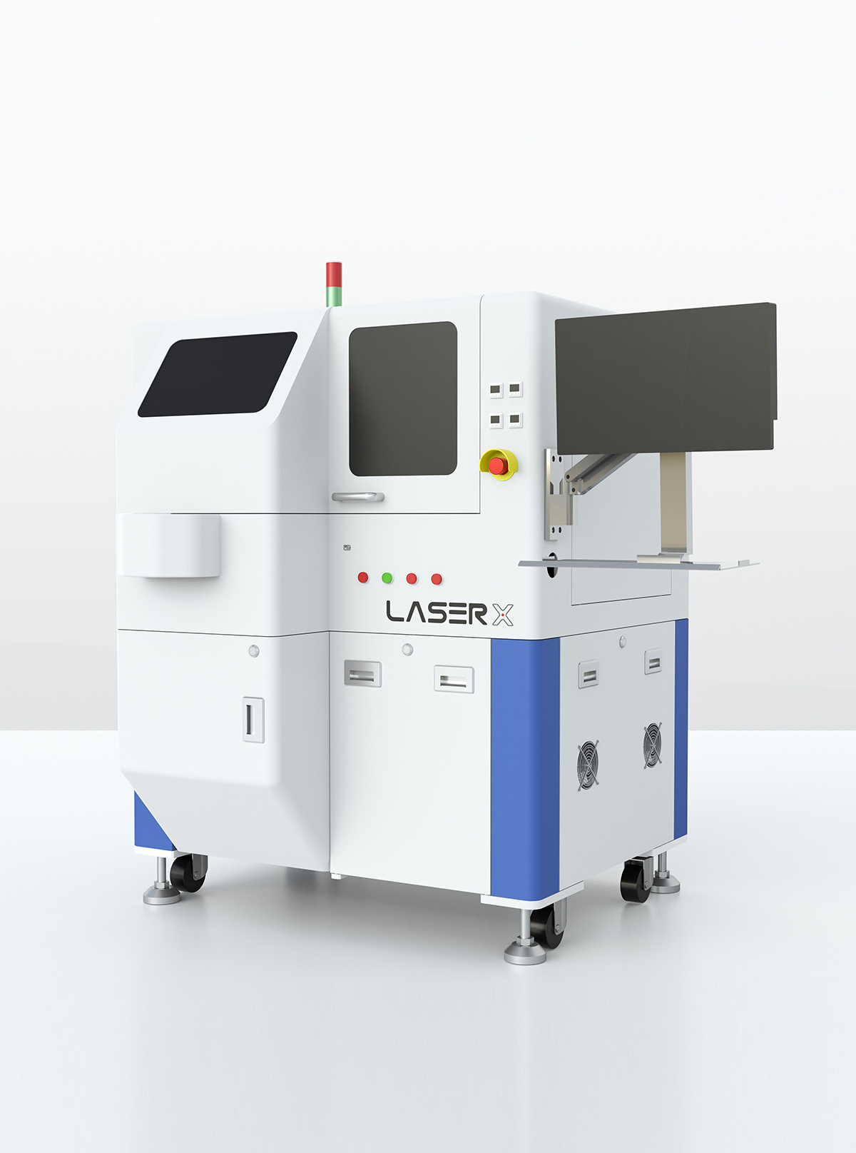
Designed for optical module/ lidar/ sensor/ SIP/ MEMS, etc., XY placement accuracy ± 3~5um@3σ

??Multi-chip bonding capability
- Auto bond-tool change, up to 4 bond-tool buffers
- Auto wafer change, up to 4 x 6” wafer ring
- Optional: Waffle pack, Gel-Pak, tray or by request
??Achieving ±3um XY placement accuracy
??Supports epoxy stamping and dispensing
??Automatic material handling system
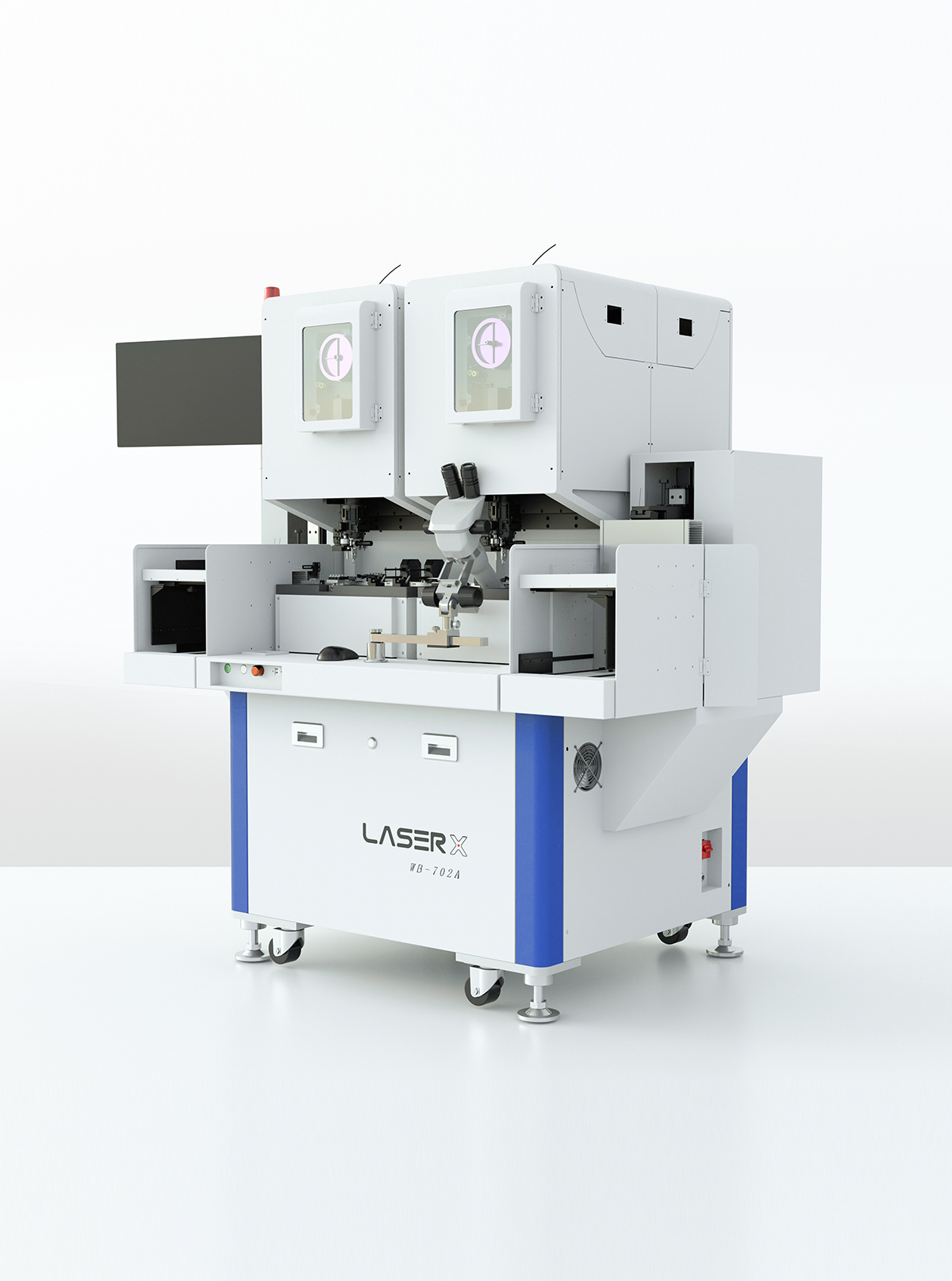
??Dual bonding head for higher production efficiency
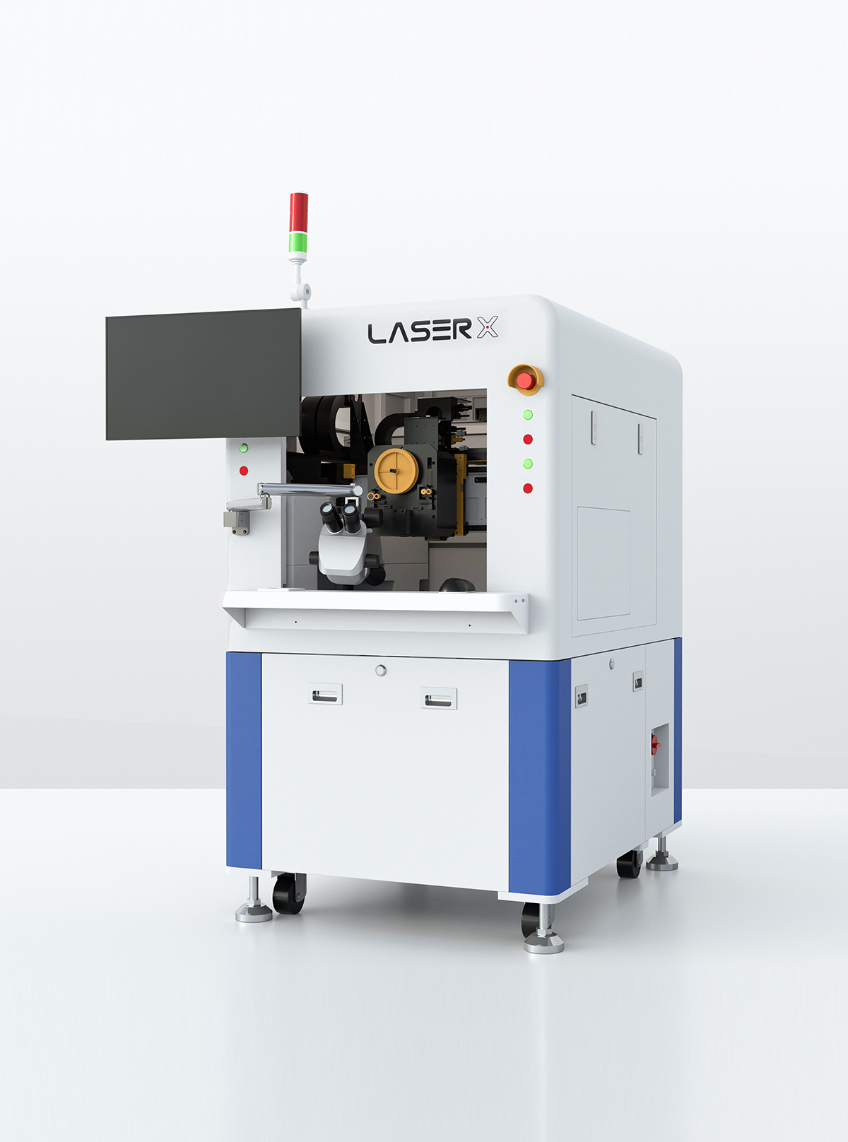
??Stable bonding force control improve bonding quality and reliability
??Programmable ultrasonic power at different stages
??Real-time bond line length detection
??Tension detection to ensure product quality
??Quickly change of ribbon wire, aluminum wire
??Long gantry XY axis for large working area
??Bond quality control and assessment
??Direct drive linear motor and flying vision systems improve efficiency
??Quickly change of ultrasonic bond head supports aluminum wire, aluminum ribbon and copper wire bonding
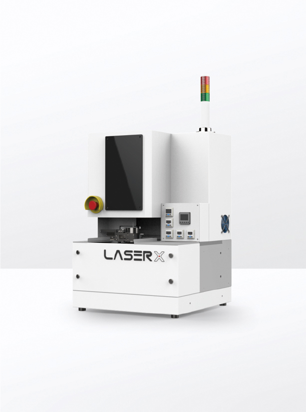
??Placement accuracy of ± 1.5 μm(3σ)
??Ability to handle tiny chips
??Apply LD and Submount cocrystal welding

 Shenzhen Headquarters:Building 3, Yufengda Industrial Park, Guangming District, Shenzhen City, Guangdong Province, China
 Reception Service Number:0755-23019639
 Consultation Email:hongbin.ding@laserx.net & laserx.xs@laserx.net
About LaserxCompany ProfileDevelopment HistoryCompany CultureHonor and Qualification
ProductsBurn-in And TesterOptical AlignmentSemiconductor PackagingChip TesterHigh precision linear and goniometer slide
SolutionSmart Factory SolutionPhotonic Assembly and AlignmentIndustrial Laser Burn-in And TesterAdvanced packaging
Copyright © 2017-2026 LASER X Technology (Shenzhen) Co., Ltd. 粵ICP備2020137519號-1